Naghmeh Bandari received her Bachelor’s and Master’s degrees in biomedical engineering from Amirkabir University of Tehran, Iran, where she served as a Certified Medical Device Technical Supervisor for six years. She is a doctoral candidate of Mechanical Engineering at the Optical-Bio-MEMS and Robotic Surgery Labs. She is also a fellow of Surgical Innovation at the Natural Sciences and Engineering Research Council of Canada (NSERC) CREATE program for Innovation-at-the-Cutting-Edge (ICE). Her research focuses on the development of optical tactile sensors and micro-optical mechanical systems for robotic and surgical applications.
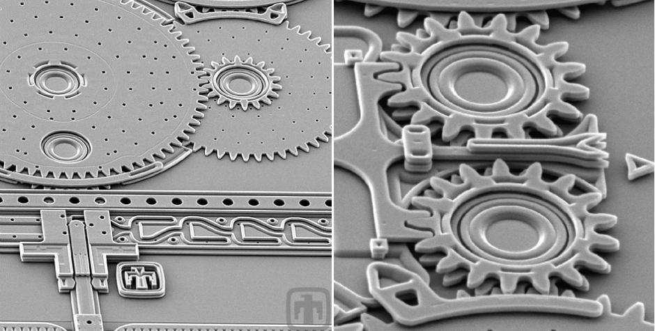
 Photo courtesy of Sandia National Laboratories
Can you imagine a pressure pump or a thermometer so small that you need a microscope to see it? Can you envision a mechanical sensor or an electrical motor smaller than a strand of hair? It's hard to believe, I agree, but it's reality!
In fact, such small compartments of electrical and mechanical systems can further an assembly of multiple other systems but still can’t be seen by the naked eye. Such small electro-mechanical integrated systems belong to a family known as micro-electro-mechanical systems or MEMS. The figure above depicts two MEMS under electron microscopy imaging.
Over the last decade, design, analysis, fabrication and development of MEMS have led to the formation of MEMS technology. MEMS technology has had a profound effect on our daily lives. For example, MEMS have significantly enhanced technologies used in the radar that’s incorporated in the adaptive cruise-controller of our cars. Another example is the development of the post delivery, surveillance and firefighter drones, which would have been impossible to create without the use of MEMS.
A very well-known application of MEMS in our daily life is the camera in our cell phones, which incorporated millions of tiny, little cameras — pixels — to freeze frame vivid images of a child’s first tooth or a lover’s smile.
The very first appearance of MEMS dates to the 1960s. However, technological limitations delayed their mass production for two decades. In the 1980s, the development of MEMS took such a pace that in less than a decade, it was known as ‘the king of technologies.’ Fast production and low costs were the main reasons for the rapid expansion of this technology in virtually every aspect of our lives.
Like macro — visible — machines, MEMS usually have two integrated components: mechanical and electrical. The electrical component can either relay or receive an electrical signal to or from an external non-MEMS receiver, like a computer, wireless network, cell phone or smartwatch. The mechanical part is responsible for sensing a mechanical parameter — temperature, pressure or force — or making a specific motion like moving a piece, opening a micro-gate or vibrating with a specific frequency.
Given that the length-scale of MEMS are in the order of one-tenth to one-thousandth of a millimetre, conventional fabrication methods like drilling, milling and turning are not suitable. Over time, experts developed very precise manufacturing techniques for MEMS. Such techniques are mainly based on electrochemical processes like etching and guided corrosion. Therefore, to have the best final product, experts can only use a few materials to make the MEMS, such as silicon wafers and resins.
One of the most common techniques for making MEMS is the utilization of stereolithography (SLA) on silicon wafers. Experts opto-chemically etch wafers with a pre-printed template and stack multiple wafers on each other to form the spatial shape of the final product. It is noteworthy that SLA is the technique used in resin-based 3D printing applications — like making jewelry — that has boomed in the last decade. Yet another application of MEMS in our daily lives.
From the 2010s, the integration of optics with MEMS opened new horizons for novel applications. For instance, optical-MEMS have made 5G communication available for us. Also, optical-MEMS have further developed advanced, faster, cheaper and more accessible medical imaging, rapid non-chemical cancer diagnoses, robotic biosensors, and even rapid pregnancy test kits.
By using light as the signal carrier medium, optical-MEMS devices are faster than their electrical ancestors. Not only are such devices faster compared to electrical MEMS, but they are also safer, cheaper and simpler in design. These properties come in handy when one needs to use a MEMS device in a biological environment, like the human body. Therefore, optical-MEMS devices have been widely exploited for surgical and diagnostic applications.
My research is in the biomedical field. Therefore, I am passionate about the applications of optical-MEMS devices in treatment, surgery and diagnostics. The primary advantage of using optical-MEMS devices is that they are small and cheap — and mass-producing wouldn’t require a huge factory. For example, for a blood test with all the measurements, an optical-MEMS blood test kit that is smaller than half a fingernail would only need one drop of blood.
Researchers have developed optical-MEMS medical devices for cancer detection, touch sensors, blood pressure sensors, DNA tests and most diagnostic tests. For example, researchers of the Optical-Bio Microsystems Lab at Concordia have used micro-manufacturing and 3D printing techniques for the development of various MEMS for early cancer detection, blood-fat level measurements, sense of touch, laparoscopic surgery and robotic surgery.
With the current pace of expansion of optical-MEMS technology into medical applications, early detection of anomalies, as well as cheap and straightforward treatment of patients, are becoming safer, faster, more reliable, cheaper and more accessible to the general public.
In the end, with the health care budget getting tighter by day, more research and development is crucial for the expansion of such reliable treatments. This will never happen without direct governmental direction and assistance, as well as private investment and support.
About the author


